Application of laser soldering technology for packaging optical communication module components
In recent years, with the rapid development of the Internet of Things and artificial intelligence application markets, big data, cloud computing, 5G, and unmanned driving application markets have brought explosive growth to data traffic. The data center Internet has gradually developed into a research hotspot of optical communication, naturally including the packaging and welding of optical modules.
The optical module is the core of optical communication. Optical modules play a very important role in fiber optic communication. Mainly completes photoelectric conversion and photoelectric conversion, converting transmitted electrical signals into optical signals. Optical signals are converted into electrical signals through optical fibers for transmission. It mainly consists of optoelectronic devices, functional circuits, and optical interfaces. Optoelectronic devices include light emitting devices and light receiving devices.
Laser Soldering Process for Optical Module Packaging
In the industry, traditional optical communication device packaging technology is usually fixed on the surface of the joint with ultraviolet glue. First, the ultraviolet glue is applied to the joint of the device, and then cured by ultraviolet lamps. This connection method has many defects, such as limited curing depth; Restricted by the geometric shape of the device; Adhesive that cannot be illuminated by ultraviolet lamps will not solidify. Not only do we need a glue device, but we also need to set up ultraviolet lamps to make the entire system more complex. Most importantly, in the actual use of the device, due to heating and other factors, there will be a slight positional deviation at the joint between the upper and lower equipment, resulting in abnormal coupling power values of the device, reduced accuracy, affecting product quality, long production cycle, and low efficiency.
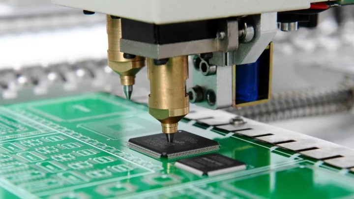
Laser solder paste welding is a very mature welding technology applied to optical communication modules. By applying solder paste on the solder pad, melting the solder paste with laser heating, and solidifying to form solder joints, the operation is relatively simple. It has the advantages of firm welding, small deformation, high precision, fast speed, and convenient automatic control, and has become one of the important means of packaging technology for optical communication equipment.
Among them, the selection of laser soldering modules, which are essential components in the field of laser soldering, is very important. ULiLASER's laser module is specifically developed for laser soldering. It is already at the forefront of the industry in terms of functionality and stability. At present, based on existing control algorithms, we have made certain progress in the experimental stage by combining AI functional algorithms. With our independently developed internal zoom lens, we have already met the application of welding different specifications of solder joints on a PCB board in a laser soldering device, which can be easily integrated with system equipment.